Device-level, not coupon-level
Characterize the device in its final package, not a test structure cut from a wafer. Real geometry, real interfaces, real heat paths.
Advanced chips fail for reasons that no single instrument can see. A thermal imager tells you where it's hot. A TDTR system tells you what a bulk material conducts. A field probe tells you where current flows. None of them tell you the full story on a real packaged device patterned, integrated, running under realistic bias conditions.
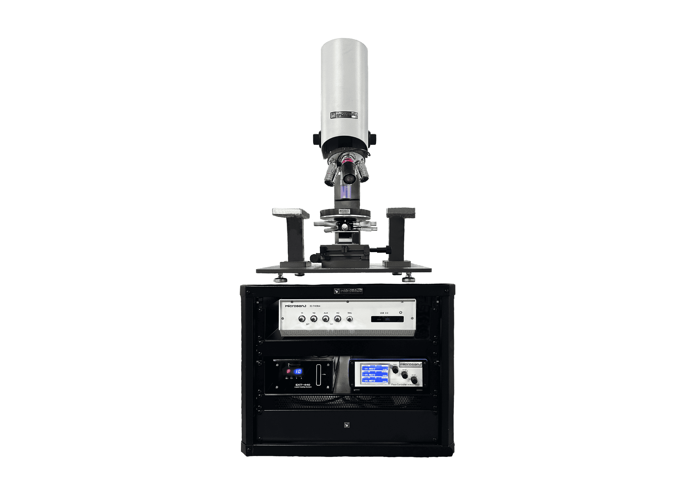
Microsanj is purpose-built to close those gaps: non-contact, spatially resolved, operating on the actual device, at the same measurement station.
Characterize the device in its final package, not a test structure cut from a wafer. Real geometry, real interfaces, real heat paths.
Every measurement is an image, not a single-point number. See where conductivity changes, where interfaces resist heat flow, where EM fields concentrate.
TR imaging has been used to validate COMSOL, ANSYS, and Beamprop thermal models across dozens of published studies. Measure first, then model with confidence.
19+
100+
20+
100+
From sub-250 nm thermal maps to wide-bandgap material conductivity to concurrent RF/EM field and thermal imaging on one integrated platform.
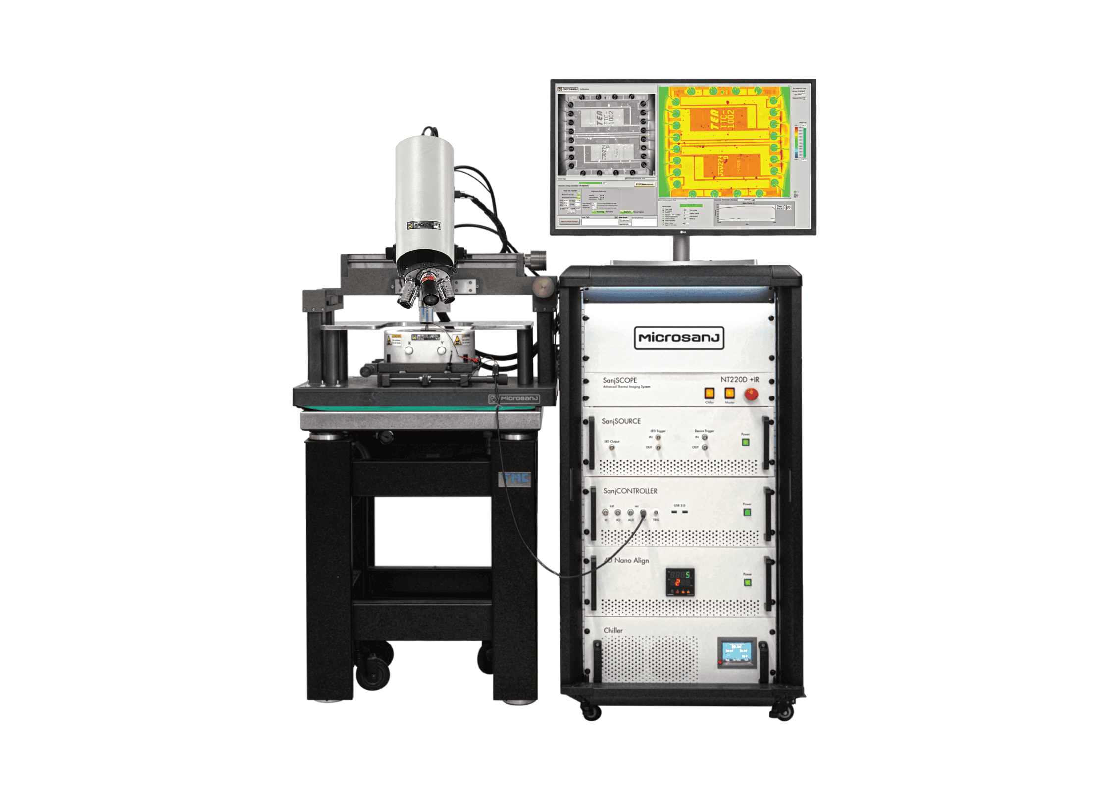
Visible-light thermoreflectance (TR) imaging delivers sub-wavelength spatial resolution and sub-millisecond time resolution on any device surface, including metals, where IR cameras produce no signal at all. Lock-in averaging achieves thermal sensitivity below 1 mK.
The platform pairs TR with dedicated LWIR infrared imaging for a complete thermal workflow: use the EZ100A-irSCOPE™ to rapidly screen a package or PCB at up to 72 mm × 61 mm field of view, then zero in on the region of interest with TR imaging at sub-300 nm resolution. Two modalities, one platform, one software environment.
Read more about the different applications →Where it's used
Where it's used
Wide-bandgap semiconductors (GaN, SiC, AlN), diamond substrates, 2.5D-3D materials, and novel dielectrics the materials driving next-generation power density require thermal property measurements that traditional test structures cannot provide on integrated devices.
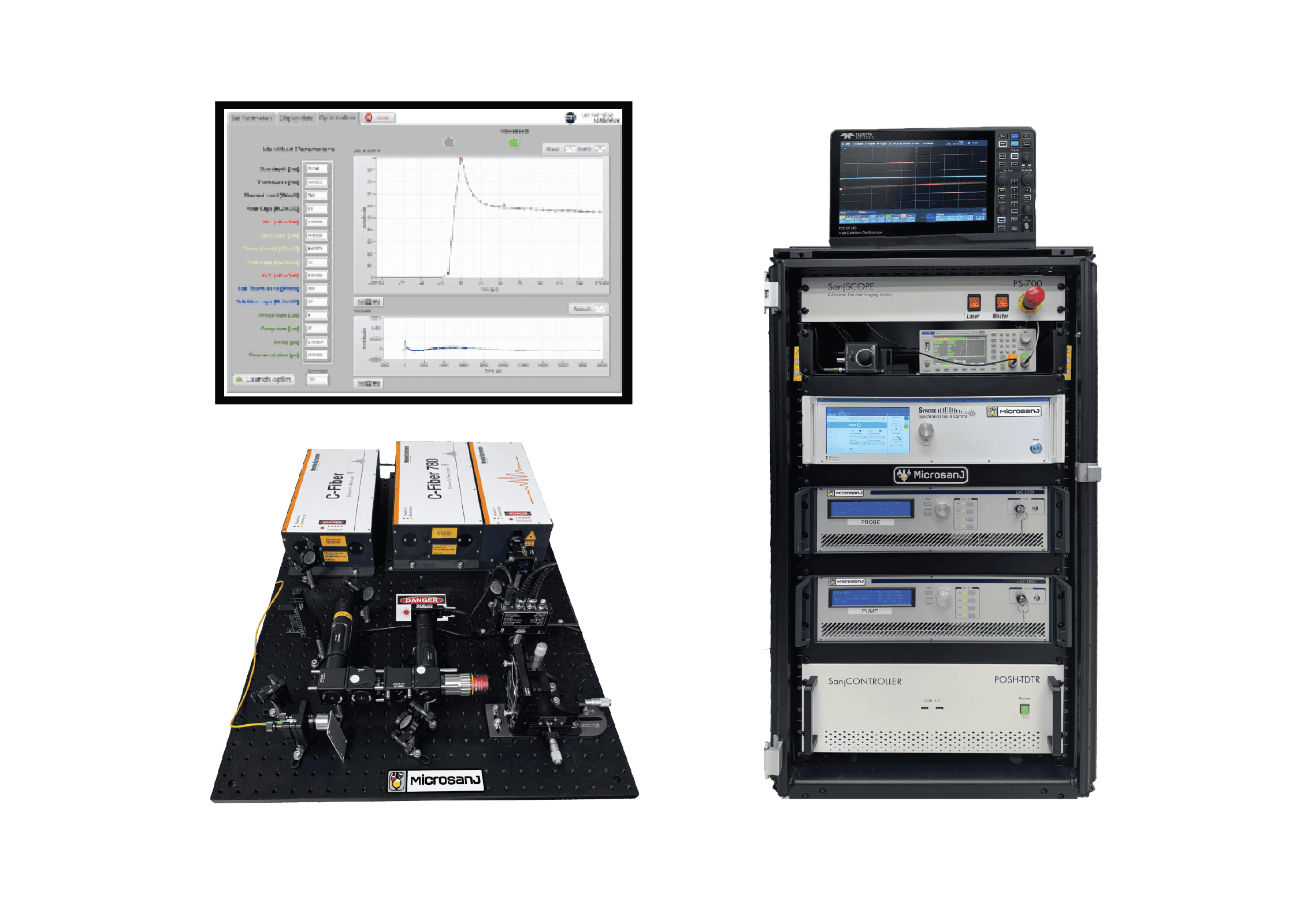
Microsanj's spatially resolved approach measures bulk thermal conductivity (κ) and thermal boundary resistance (TBR) at heterogeneous interfaces on the actual device, not a polished bulk coupon. Conductivity range spans 0.1 to 1000 W/m·K, covering insulators through diamond.
The technique builds on the TDTR (time-domain thermoreflectance) heritage pioneered at the University of Illinois at Urbana-Champaign, extended to patterned, packaged devices where academic TDTR setups cannot operate.
Materials characterization applications →Modern RF and power devices fail at the intersection of thermal and electromagnetic phenomena: current crowding, substrate coupling, and field-induced heating that no single measurement captures alone. The Microsanj platform integrates concurrent RF/EM field and thermal imaging on the same device, at the same operating point.
The emVIEW™ system, developed in partnership with the University of Wisconsin, extends the platform into quantitative RF/EM field measurement, mapping the electric and magnetic near-fields that drive the thermal behavior, not just the resulting temperature distribution.
RF/EM and 5G/6G applications →Where it's used
Start with the configuration you need today. Add materials characterization or upgrade your system without starting over your investment carries forward.
Whether you're characterizing a GaN transistor, measuring TBR in a diamond substrate, or correlating EM fields with thermal runaway, the Microsanj platform has a measurement path for it. Talk to our applications team.