
Singapore
DEC 1–4, 2026
EPTC 2026
Sands Expo & Convention Centre
Learn More
The only commercial platform that combines thermal imaging, materials characterization, RF, and EM field imaging for advanced semiconductor devices, from picoseconds to DC, and from surface to buried structures.




Microsanj proudly serves a diverse range of customers worldwide.










No other commercial system bridges all three domains. Together, they enable the multiphysics understanding of device performance that single-domain tools can never provide.
Full-field thermoreflectance imaging of operating devices. Sub-micron spatial resolution. Nanosecond-to-picosecond temporal resolution. IR + TR dual mode from macro hotspot location to sub-micron zoom.
In-plane and cross-plane thermal conductivity. Thermal boundary resistance. Thin-film analysis from 10 nm to hundreds of microns on the actual device stack, not a proxy. NOSH-TDTR + POSH-TDTR.
Together, you can perform multiphysics analysis of device performance, correlating thermal, electrical, and RF behavior on the same device. emVIEW™ extends this to near-field EM mapping without an anechoic chamber.
Different challenges. Adaptable for multiple industry solutions.






When devices fail or thermal models are wrong, it's rarely because of what you measured. It's because of what you couldn't.
Configurable architecture. Buy what you need now. Upgrade as your application evolves.
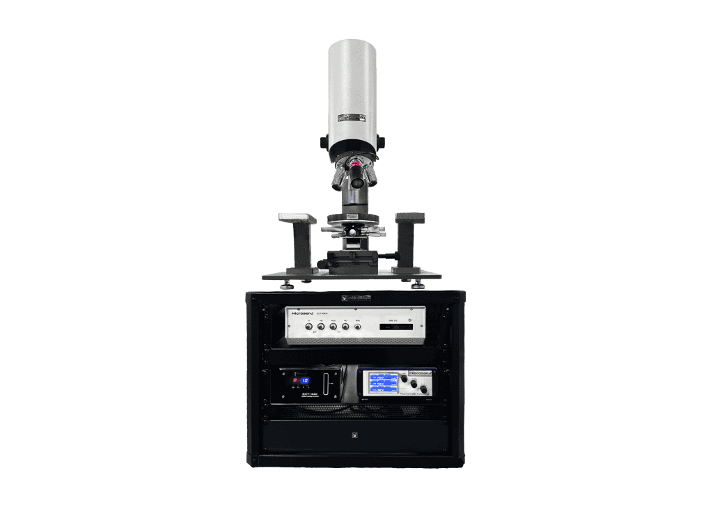
Active device R&D and production. Dual mode Thermoreflectance + IR. Up to 3 sensors.

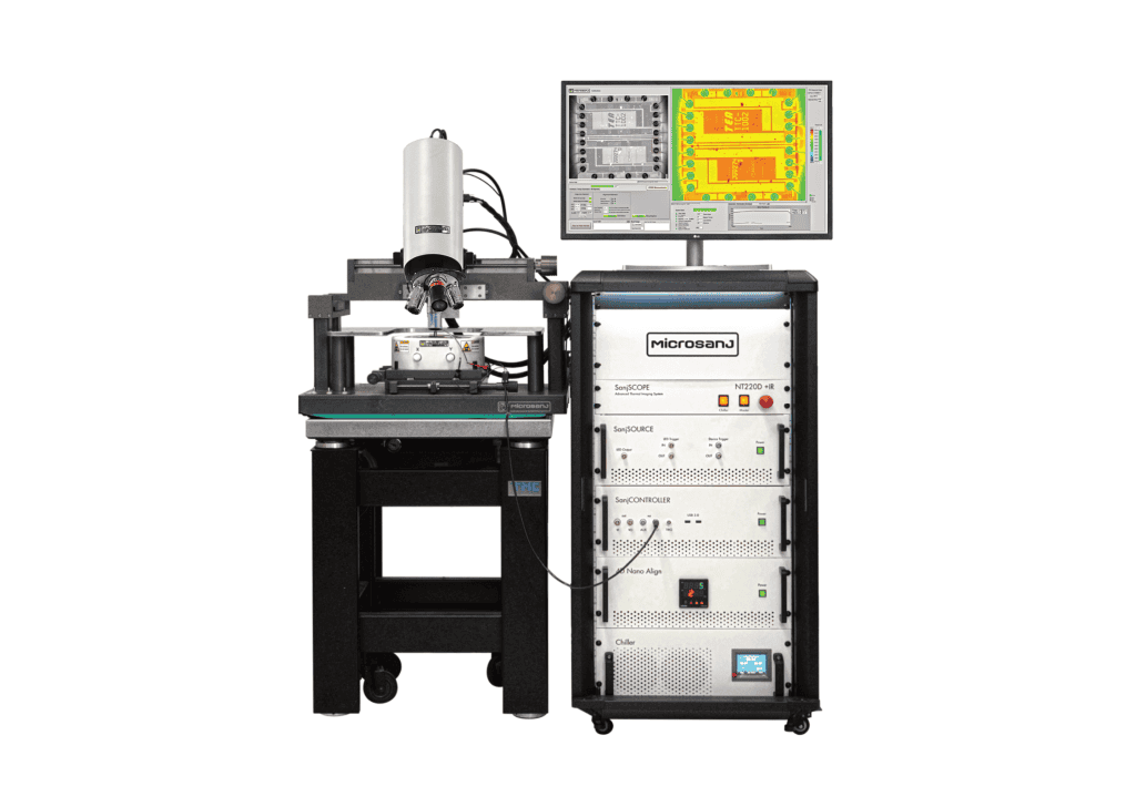
Active device R&D and production. Dual mode Thermoreflectance + IR. Up to 3 sensors.

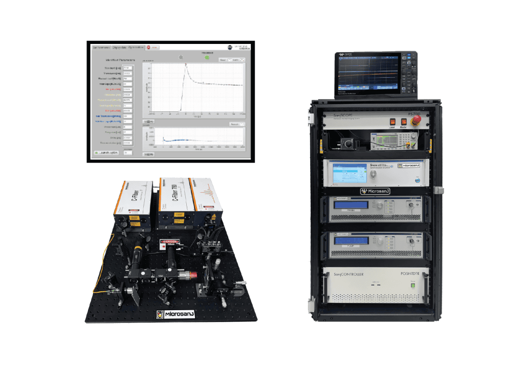
Nanosecond and Picosecond pump-probe for anisotropic material thermal properties. The gold-standard TDTR technique has been commercialized.

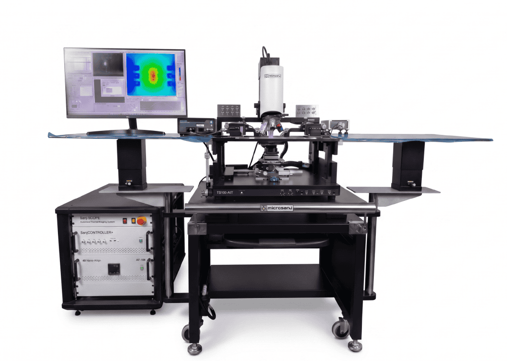
Extend your existing measurement infrastructure, MPI probe stations, RF/load-pull systems, pulsed-IV, and EM test setups with synchronized thermal and EM field imaging. No rip-and-replace. Your tools, with a new dimension of data.

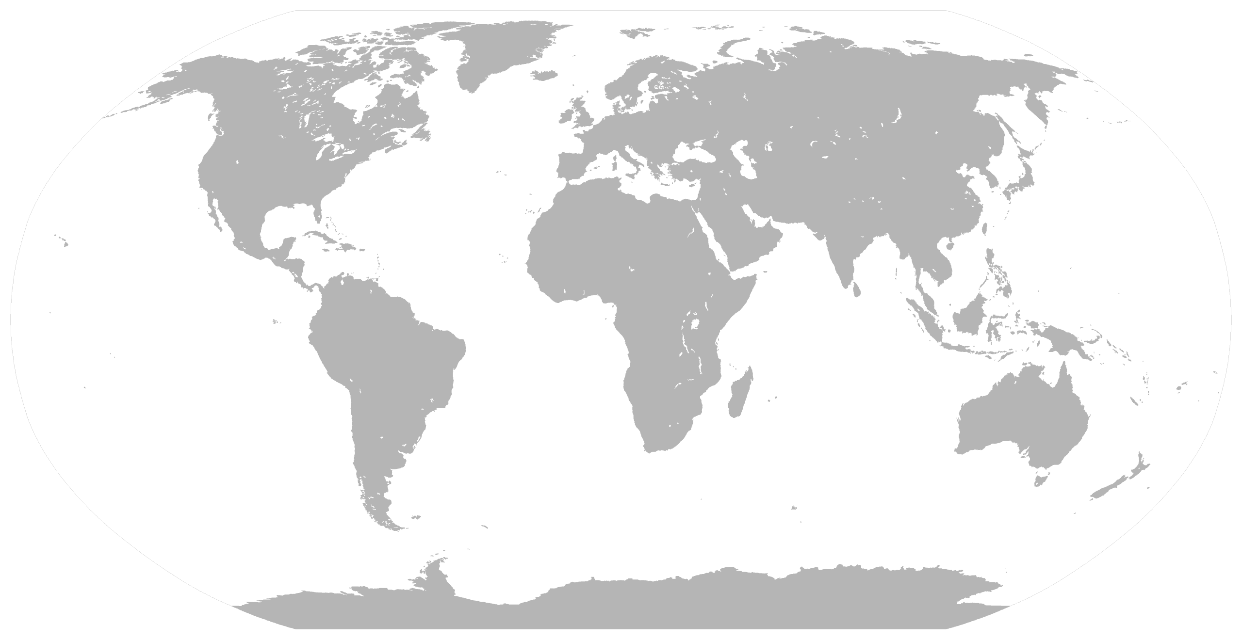
Advanced thermal imaging & materials characterization solutions trusted by researchers, engineers, and manufacturers worldwide. With distributors and sales representatives across North America, Europe, and Asia, our global team is ready to support your characterization needs from semiconductors and RF to photonics, AI, and quantum computing.

Send us your sample. We'll run a complimentary measurement. No commitment required.


See inside. Measure everything. The only commercial platform for thermal imaging, materials characterization, and multiphysics + EM field imaging for advanced semiconductor devices.
48421 Milmont Dr.
Fremont, CA 94538
+1.408.256.1255
Hours: 8:00am - 5:00pm PST M-F
See how our thermal, materials characterization, and multiphysics + EM field imaging platform performs on your advanced semiconductor devices. Book a live demo with one of our engineers.

Copyright © Microsanj LLC - 2026